 Home
Home


Making a PCB
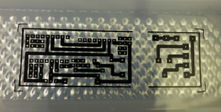
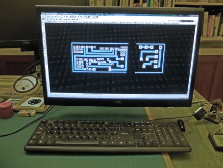
Stage one: the circuit is designed on the computer. I am using free Design Spark from RS Components. The design is printed out using an inkjet printer at best quality available on special clear film sold for the purpose by Rapid Electronics.
I print out two copies and tape them together to ensure the maximum density. This may not be necessary but I have always done this ever since I was using a dot matrix printer on tracing paper!
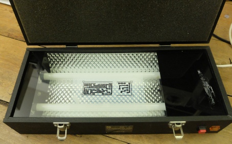
Stage two: the design goes, printed side up, in a uv light box which I bought second hand on Ebay.
(It’s a good idea to warm up the lamps for a couple of minutes before exposing the PCBs to ensure the lamps are emitting their full intensity from the start.)
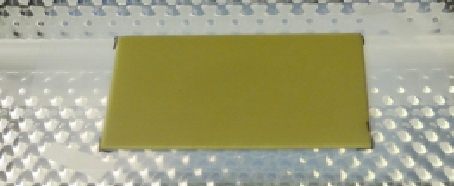
Take a piece of photosensitive PCB material (I use a band saw to cut it to size -
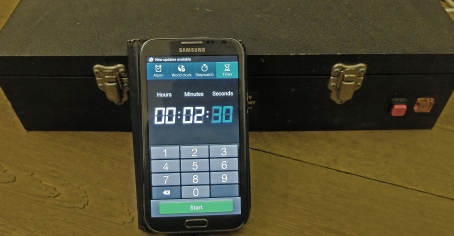
Close the lid and turn on the lamps. I find 2 minutes 30 seconds works ok but there is a wide margin of error. (Don’t expose yourself to the lamps -
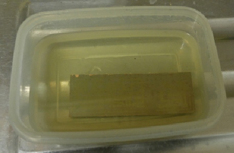
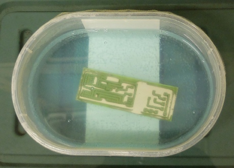
Stage three (above): place the PCB in developer solution made up to the manufacturer’s instructions. I use ice cream containers or similar. (I get my chemicals from Rapid Electronics). The solution should not be hotter than about 18 degrees Celsius otherwise the developing process is very rapid (seconds) and may go too far and strip off all the photo resist. I take the PCB out during this process and rinse it and then examine it carefully to see how far along the process is. Rinsing seems to slow the process down and give you time to check on progress. The PCB should remain in the liquid until all traces of discolouration have gone from the areas to be etched (the bare copper should be really bare -
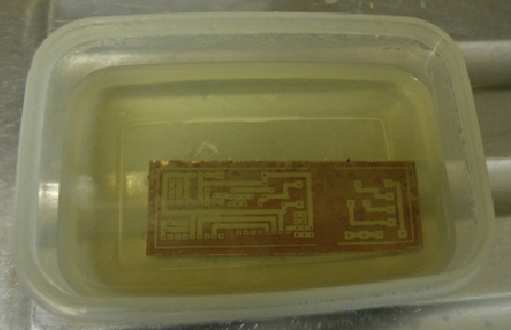
When you are satisfied the PCB is fully developed, rinse it thoroughly, ready for etching.
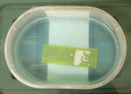
It will look something like this.
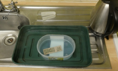
Stage three: place the PCB in the etchant solution. This should be hot otherwise the process will take hours instead of about fifteen to twenty minutes. I keep the solution hot by adding boiling water from a kettle to the tray in which the PCB and the etching solution is placed. Holding the PCB with tweezers and moving it back and forth speeds things up by getting rid of bubbles which form during the chemical action and ensuring that the solution close to the copper does not get depleted.
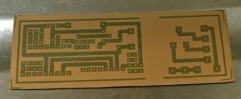
As shown below, the copper gradually dissolves.
(Keep the chemicals clear of food! I’m fortunate to have a utility room to do these things in -
When the process is complete, rinse thoroughly.
The remaining resist can be removed by placing the PCB in hot developer or by rubbing with a damp Scotch pad. Do this before you drill as the slight burrs raised by the drill make it more difficult to clear all the resist.
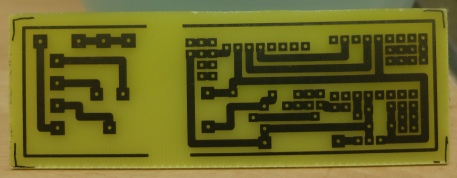
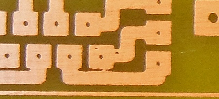
It’s very easy to make a basic single-
When designing a PCB, I try to keep everything as big as possible (relatively). Tracks as wide as can be accommodated and pads square, and again, as big as possible. Although it’s quite possible to produce reliable tracks of say 15 thou width, I find the limiting factor is hand drilling holes. I generally limit myself to 1mm drill bits which require a pad side of about 90 thou (square). So I’m really talking about using old-
Also large tracks and pads conduct heat away better and etch quicker (the more copper you remove, the more quickly your chemicals will be used up! If you want to connect automotive size wires to the PCB, you are going to need 2 or 2.5 mm holes and pads say 130 thou square. Remember, any strain on the pads from connections could tear the copper off the substrate if the pad is too small.
By the way, when working with chemicals which are required in this sort of PCB manufacture, use blue nitrile gloves, plastic tweezers and goggles. In my youth, I used to do a lot of photographic processing and would happily dip my hands in all sorts of chemicals. I have learnt better since I hope!
The making process
Check for problems like this where all the resist didn’t clear during development. In this case, careful use of a Stanley knife could probably solve the problem.

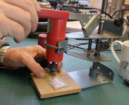
Stage four: use a small craft drill in a stand (Expo or similar -
I keep an eye and ear out for a blunt drill bit which takes too much time and pressure to get through, raises a high burr and may wander from the correct position. Carbide tipped are the ones to go for, high speed steel bits last for one big PCB only.
I use a head magnifier and an LED lamp to enable me to see what I’m doing and just aim for the centre of the holes. The holes act as a guide and the vast majority if the time the holes go in the right place!
by using a photo-
Historical note here…
Useful materials from Rapid Electronics
Ink jet film: Jetstar standard, Mega Electronics, 39-
RVFM Photo etch PCB, 34-
PCB fine etch crystals, Mega Electronics, 34-
Liquid developer concentrate, Mega Electronics, 34-