Home Julian Rogers Home How to make a PCB

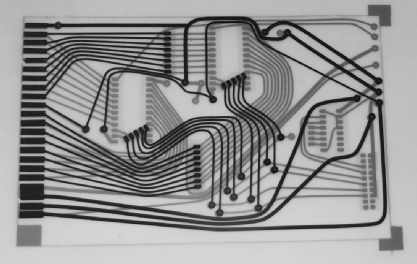
PCB design I did in the early nineties for a two sided design using self-adhesive graphics art tapes. These could be obtained in various widths and were crepe-type which could be bent to shape. You worked over a 100 thou grid and cut the tape as required with a scalpel. Pads were available on backing paper so the could easily be laid into position. Also groups of pads in various configurations for ICs etc. Pads went down first then connections just overlapping the pads.

When getting dense enough printing to block uv could be a problem, at least this was totally opaque. Also the gentle curves are rather aesthetically pleasing!

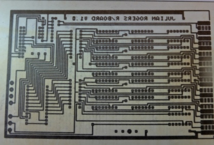
Here’s a design from the mid eighties (I used EasyPC I think). It’s printed out on some sort of tracing paper. I can’t remember how this was printed out. Probably dot matrix.

I seem to remember trying to over-print the design a second time to improve the density but alignment in the printer was problematical. Two designs taped together worked. I sometimes inked in problematical areas with a fine ohp pen.

On this one, the printing seems to have failed on the edge connectors on the right.

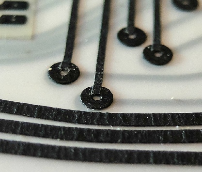
The crepe nature of the tape shows up here.

My old PCBs